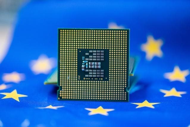
February 9, 2026: The EU inaugurated NanoIC, Europe's largest Chips Act pilot line, at IMEC's Leuven campus. Total investment: €2.5 billion (€700M from EU, €700M from national/regional governments, remainder from ASML and partners).
The facility focuses on beyond-2nm chip development—cutting edge of semiconductor technology. It's the first European site to deploy ASML's most advanced High NA EUV lithography machine.
Executive Vice-President Henna Virkkunen, Belgian Prime Minister Bart De Wever, and Flanders' Minister-President Matthias Diependaele cut the ribbon. ASML CEO Christophe Fouquet showed up too, which makes sense given ASML's equipment is kind of the whole point.
The pitch: open access pilot line where startups, SMEs, researchers, and large companies can test next-gen chip designs before committing billions to mass production.
The reality? Well, let's look at what this actually means.
What NanoIC Actually Is
Not a commercial fab. Not a factory that produces chips at scale. A pilot line—think prototype facility.
Purpose: Bridge the gap from "lab to fab"—testing processes, equipment, and designs at near-industrial scale before companies invest $15-20 billion in full production facilities.
Which is useful, don't get me wrong. You don't want to drop $20 billion on a fab only to discover your 2nm process doesn't actually work at volume.
Technology: Beyond-2nm system-on-chip (SoC) development, targeting AI accelerators, 6G comms, autonomous vehicles, healthcare applications.
Partners: Hosted by IMEC (Belgium), with CEA-Leti (France), Fraunhofer (Germany), VTT (Finland), CSSNT (Romania), Tyndall National Institute (Ireland).
Capacity: 12,000+ square meters of cleanroom space now, with 4,000 more under construction. Over 100 new tools being integrated over five years.
It's part of a network of five pilot lines (NanoIC, FAMES, APECS, WBG, PIXEurope) representing €3.7 billion in combined EU and national investment.
FAMES opened January 30, 2026. NanoIC follows two weeks later. So the infrastructure is real and operational, which is more than you can say for a lot of EU initiatives that get announced and then quietly disappear. I'm looking at you, various digital sovereignty projects.
The Broader Chips Act Context
The EU Chips Act launched in 2022, entered force September 2023, with a stated goal: double Europe's share of global semiconductor production from 10% to 20% by 2030.
Total committed funding: approximately €43 billion (public and private combined).
Three pillars:
- R&D and innovation (pilot lines like NanoIC)
- Capacity building for large-scale fabs
- Crisis preparedness and supply chain monitoring
So far, the EU has approved seven state aid decisions for semiconductor facilities representing over €31.5 billion in total investment:
- Intel: €30B fab in Magdeburg, Germany (backed by €11B German subsidies)
- ESMC (TSMC/Bosch/Infineon/NXP joint venture): Dresden fab, Germany
- STMicroelectronics: Italy facility for Silicon Carbide production
- GlobalFoundries/STMicroelectronics: France fab (€8.13B French subsidies)
And more in the pipeline. The money is flowing, at least on paper.
Who This Affects
European startups and SMEs: Gain access to beyond-2nm process design kits without building their own fabs. That's genuinely useful—entry barrier to advanced chip design is massive otherwise.
Research institutions: Can test concepts at near-production scale. Universities across six countries get access to cutting-edge tools.
Equipment manufacturers: ASML gets to deploy High NA EUV in European territory, creating local expertise and potentially future customers.
Foundries and IDMs: Can test new processes before internal investment. Intel, TSMC partners, GlobalFoundries all benefit from de-risked R&D.
European automotive/telecom/healthcare sectors: Industries dependent on advanced chips get potential local supply chain resilience. Maybe.
Who This Doesn't Affect (Yet)
Nvidia, AMD, TSMC's core business: NanoIC is R&D infrastructure. It's not competing with TSMC's 70% foundry market share or Nvidia's 92% GPU dominance. Those companies operate at volume production scale—millions of wafers per year.
NanoIC's role is upstream: developing the processes that could eventually get used in commercial fabs, assuming everything goes according to plan.
Consumer hardware prices: Zero short-term impact. Pilot lines don't produce retail products. They test concepts. Your RAM isn't getting cheaper because Belgium opened a research facility.
Global semiconductor oligopoly: TSMC still controls 70% of foundry capacity. Samsung, SK hynix, Micron still control ~70% of DRAM. Nvidia still owns 92% of discrete GPUs. NanoIC doesn't challenge any of that market power. Like, at all.
Memory/GPU shortages: NanoIC won't produce a single stick of RAM or graphics card. It's focused on logic chips (AI accelerators, automotive processors, telecom chips), not memory or consumer GPUs.
The Geopolitical Play
Here's what this is really about: Europe currently manufactures almost zero cutting-edge chips. TSMC (Taiwan) produces 90% of advanced semiconductors. That's a strategic dependency problem.
When Trump floated 25% tariffs on semiconductor imports, companies panicked. When China threatens Taiwan, everyone worries about chip supply. Europe noticed it has no domestic capacity for the chips that run AI data centers, autonomous vehicles, or military systems.
The Chips Act is industrial policy dressed as economic development. It's about:
- Reducing reliance on Taiwan (geopolitical risk)
- Reducing reliance on US firms (strategic autonomy)
- Preventing China from dominating future chip technologies
- Maintaining European equipment manufacturer relevance (ASML)
CSIS analysis notes: "Neither the US nor EU has capability to manufacture at scale the most advanced semiconductors... that capability resides mainly in Taiwan."
Translation: Europe is trying to build domestic capacity for technologies it currently imports entirely.
The Competition Question
Will NanoIC hurt Nvidia, Intel, TSMC? Not directly, and maybe not at all.
Intel: Actually investing €30B in Europe (Magdeburg fab). They're collaborating, not competing. Intel needs European subsidies; Europe needs Intel's manufacturing expertise. Mutually beneficial.
TSMC: Already partnering on ESMC Dresden fab. TSMC is cautious about European expansion (labor costs, regulatory complexity), but they're not threatened by a pilot line. Volume production is their moat.
Nvidia: Buys from TSMC. If Europe eventually produces competitive foundry capacity, that's more supplier optionality for Nvidia, which they'd probably welcome. But that's 2030+ scenario, not 2026 reality.
ASML: Benefits directly. High NA EUV deployment in Europe creates local expertise, strengthens ecosystem for their equipment. This is good for ASML.
The real competition isn't company vs company—it's US vs EU vs Asia for semiconductor capacity allocation.
And on that front, Europe is still way behind. TSMC produces 70% of foundry output. Europe produces... a rounding error.
Does the 20% by 2030 Goal Matter?
The EU wants 20% of global semiconductor production by 2030. Currently: ~10%.
Sounds achievable. Doubling from 10% to 20% in eight years (2022-2030).
But here's the issue: "global semiconductor production" is a meaningless metric for strategic autonomy.
Interface EU analysis points out: Different chips require different fabs. An advanced AI accelerator fab can't produce power semiconductors. A memory fab can't produce logic chips. A 2nm node facility can't make 180nm automotive chips.
Europe could hit 20% total capacity while still having zero domestic capability for the specific chips that matter strategically (advanced AI, military processors, cutting-edge automotive).
Even Europe's Court of Auditors notes: "Pillar II uptake is slow and unlikely to be sufficient for the 20% target by 2030."
Translation: The big commercial fabs aren't being built fast enough. Intel's Magdeburg is delayed. TSMC is cautious. Most investment is in older nodes or niche applications, not bleeding-edge manufacturing.
What Actually Matters Here
Forget the 20% target. That's political window-dressing.
What matters:
- Talent development: Training European engineers on beyond-2nm processes
- Process development: Creating pathways from research to production
- Ecosystem building: Connecting startups, researchers, equipment makers, and manufacturers
- Strategic capability: Ensuring Europe can produce critical chips if global supply chains break
NanoIC addresses #1-3 effectively. It's good infrastructure for R&D.
It does almost nothing for #4 in the short term. Pilot lines don't produce volume. Commercial fabs do, and those take 3-5 years to build, cost $15-20B each, and require sustained commitment.
Europe has approved €31.5B in fab investments. That's substantial. But for context: TSMC alone spent $36B in capex in 2023. One company, one year.
Europe's catching up from a standing start. Progress is real but the gap remains enormous.
My Assessment (Opinion, as in my own )
NanoIC is actually good infrastructure. Open-access R&D facilities matter, especially when they give startups and researchers access to beyond-2nm tools without requiring billions in capital investment. That genuinely creates innovation potential.
But we need to be realistic about what this solves—which isn't much beyond "Europe now has excellent research facilities."
From the info I got when writing another article, which I will be publishing soon—TSMC 70%, Nvidia 92%, memory controlled by three companies—NanoIC doesn't touch any of that. This is R&D infrastructure. The market concentration that's squeezing consumers and enabling AI companies to monopolize DRAM supply? Unchanged. Still broken. Still expensive. Still controlled by the same players.
Will NanoIC eventually contribute to more competitive semiconductor manufacturing in Europe? Maybe. In 2030+. If the commercial fabs actually get built. And if companies choose to use European capacity instead of just going to TSMC like everyone else because why wouldn't they.
That's a lot of ifs for €2.5 billion.
Here's my actual concern: Europe is building pilot lines while the US and Asia build volume production. Intel's getting $6.6B from the US government for Arizona fabs. TSMC is expanding in Taiwan and Arizona. Samsung's building in Texas. China is throwing hundreds of billions at legacy nodes.
Europe's strategy is "collaborate and specialize" rather than "build everything." That's probably smart given resource constraints. But it also means Europe remains dependent on others for volume production.
Which is fine, I guess, if global supply chains never break and geopolitics stays stable forever. Anyone want to take that bet?
The CSIS report notes that US and EU Chips Acts both "call for international collaboration with allies and partners" because neither can compete with Taiwan/Korea alone.
Translation: Even with €43B in funding, Europe can't achieve semiconductor independence. Best case scenario is reducing dependency while maintaining equipment leadership through ASML, maybe developing some niche capabilities for specific applications.
Which is progress, sure. But let's not call it sovereignty. That's marketing.
The honest version of the Chips Act would say: "We're trying to go from 100% dependent on Asia/US to maybe 70% dependent by 2030, with domestic capacity for some strategic applications."
Instead we get "20% of global production!" which sounds impressive but obscures what's actually being built. It's the kind of metric politicians love because it's technically true while being functionally misleading.
In every article something bothers me, so here, the issue is about the framing: Pilot lines are important. R&D infrastructure matters. But calling this "Europe's largest Chips Act pilot line" makes it sound like major progress on semiconductor independence when it's really just... a very nice research facility that won't produce a single commercial chip.
The real test: In 2030, can Europe produce its own AI accelerators, automotive processors, and defense chips at volume without relying on TSMC/Samsung/Intel?
Based on current trajectory: No. Or very limited volumes for specific applications. The big commercial fabs (Intel Magdeburg, ESMC Dresden) are the actual determinants, and those are delayed, undersized compared to Asian capacity, or partnered with non-European firms anyway.
I keep coming back to the scale problem. TSMC produces 480,000 wafers per month at a single fab. They operate multiple fabs. Intel's Magdeburg will target similar scales but won't be operational until late 2020s.
Europe is announcing €2.5B pilot lines while TSMC spends $36B annual capex on production capacity. The difference is absurd when you actually look at the numbers.
But….and this matters, building R&D infrastructure is the necessary first step. You can't have commercial fabs without process development. NanoIC creates the knowledge base for future European manufacturing.
It's just going to take a lot longer than 2030 to matter. Like, possibly 2035+. Maybe 2040 if we're being honest about fab construction timelines and geopolitical delays.
Personal take: This feels like Europe playing the long game while hoping global supply chains don't collapse in the meantime. The infrastructure is real, the investment is substantial, the technology access is valuable.
But if Taiwan gets blockaded or TSMC's Arizona fabs get delayed or memory prices spike another 172% because three companies control supply... NanoIC won't solve any of that. It'll just be a really nice research facility that trained some engineers who then got hired by TSMC Taiwan because that's where actual production happens.
Look, foundations are necessary. But you can't build a strategy on foundations alone when what you actually need is production capacity.
Sources: European Commission (Chips Act announcements), IMEC press releases, Reuters, The Next Web, Evertiq, Techzine Global, CSIS (semiconductor policy analysis), Interface EU (Chips Act critique), European Court of Auditors (Special Report 12/2025), TrendForce, Wikipedia (semiconductor market data)
Note: Market share figures, investment amounts, and capacity data from official EU announcements, company filings, and industry analysts. Strategic assessment based on policy analysis from CSIS, Interface EU, and European Court of Auditors reports. Opinions on effectiveness and timeline are analytical interpretation.